The Beginner’s Guide to BGA: What Is It?
BGA stands for “Ball Grid Array.” BGA packages allow for connections with high density to be enabled and made more efficient to integrated circuits (ICs). To do so, the underside of a chip package is utilized to make the connection.
In the past, connections were made around the edge. Using the IC package's underside allows for the connection density to be reduced, which helps streamline or simplify the layout of printed circuit boards (PCBs).
However, the use of SMD (surface-mounted device) BGA packages do come with certain drawbacks. Utilizing the underside of the chip will ensure that trying to obtain direct access to the connections will be rendered impossible. As a result, inspections, desoldering, and soldering will be far more difficult to achieve.
Fortunately, advances have been made in the PCB field, and mainline printed circuit board production apparatuses have been able to bypass such issues. In fact, they can do so while also augmenting performance and reliability properties in the process. Here, however, our focus will be on the BGA process and the main reasons it is used.
Why is BGA used?
BGA is a very straightforward process, which is antithetical to many of the other technologies available. For the longest time, the quad flat pack (QFP) style package was seen as the gold standard. However, its pins were not only very closely packed together but also very thin. As such, many difficulties arose that led to downtime and other issues.
For example, they would often become damaged, as QFP pins are quite thin, and the way that they are spaced necessitates positioning that has to be very prudently controlled. Even seemingly minor mishandling can lead to mass displacement, which would render restorations null and void.
Furthermore, integrated circuits that use very high pin counts also tend to cost significantly more than their low pin counterparts, which can further exacerbate the problem.
Pin density is another issue, as pin density, at least from a design standpoint, was such that removing tracks from the integrated circuit would become a serious issue because congestion would result in certain areas.
Soldering is another problem to consider, as very prudent controls had to be initiated when soldering took place due to the QFP pins being very closely set together. Otherwise, the contacts can be bridged with relative ease, so careful control of the soldering process needs to be implemented.
In sum, BGA was developed to overcome all of the issues above. BGA was also devised to enhance the reliability of the soldered joint. Due to its myriad benefits, BGA is commonly used today in many countries. Various equipment and processes have been modified or augmented to overcome some of the issues that BGA use presents.
The Aim of BGA
BGA was created to provide a variety of benefits to the end-users of equipment, the manufacturers of said equipment, and a bevy of benefits to integrated circuits themselves. Below are just some of the benefits that BGA provides vis-a-vis other alternative technologies.
For starters, BGA allows for the highly efficient use of PCB space, which facilitates connections that can be made underneath the SMD package itself. In the past, connections could only be made around its periphery, so many manufacturers have seen this change as a significant improvement.
Moreover, electrical and thermal performances have also been augmented drastically due to BGA, as BGA packages offer both ground and power planes for low inductances. As well, they provide impedance traces for signals that are highly controlled. BGA packages can also route heat away by taking advantage of the pads.
BGA soldering in Toronto has also been improved, which allows for drastic improvements in manufacturing yields. In other words, BGA allows for wider spaces to be made between connections, and its use helps improve the overall level of soldering.
Reduced package thickness is also facilitated thanks to BGA, which is an absolute must when several assemblies need to be made far thinner than normal, as is often the case with mobile phones. Another advantage of BGA is that its larger pad sizes help ameliorate re-workability.
What exactly is a BGA package?
BGA uses a very different approach to the connections when compared to the approach used for more typical surface mounted connections. For example, quad flat packs would use the sides of the package to make the necessary connections.
As a result, there was very limited space for the pins, which forced manufacturers to make their pins smaller than normal and pack them very close to one another to meet connectivity requirements.
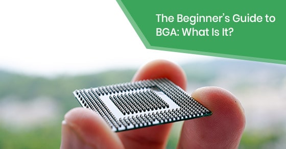
Fortunately, the BGA package provides far more space with which to work, as the entire underside of the package can be utilized to make the necessary connections. As for the pattern itself, the reason why BGAs are referred to as “Ball Grid Arrays” is that the pins are set in a grid-like pattern on the carrier's underside.
It should also be noted that pins are not used with BGA packages to provide the necessary connectivity. Instead, pads that come equipped with balls of solder are utilized to form the connection.
As for the PCB onto which the BGA unit is to be set, there is a matching set of pads made with copper that is used to facilitate the connectivity.
Circuits Central
If you would like to learn more about BGA soldering or require BGA soldering in Toronto from a reputable and reliable manufacturing company, then please visit our website. We can also be reached at 888-821-7746 if you want to learn more about our excellent prototyping, PCB manufacturing, and electronics services.