
Why Your Prototype Passed and Your Production Run Didn’t
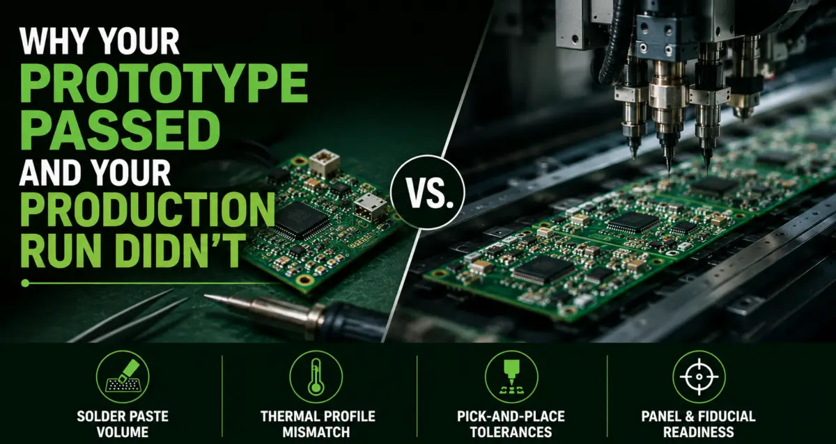
The prototype worked. Functionality was confirmed. Tests passed. You signed off on the design and handed it to your contract manufacturer for volume production. Then the failure reports started.
This is one of the most consistent and expensive surprises in electronics development. Many first production runs reveal manufacturability gaps that prototype builds never exposed, with rework costs and schedule delays stretching four to eight weeks or more when process incompatibilities surface at scale. The root cause is almost never a flawed circuit. It is a design that was validated under conditions that do not reflect what happens inside a volume assembly line.
When "Works on My Bench" Is Not Enough
Prototype builds and production runs are not the same process. Prototype boards are often hand-assembled or built through selective soldering with close manual oversight. Adjustments happen in real time: a technician repositions a component, adds a touch of flux, or corrects a reflow temperature when a joint looks suspect. These interventions produce a working board, but they mask conditions the design has not actually solved.
Volume production removes every one of these human interventions. Automated pick-and-place machines operate within fixed tolerances. Solder paste is deposited through framed stencils with aperture geometries calibrated to control paste volume precisely. A single reflow profile carries every board through the oven identically. Anything the prototype survived through manual correction becomes a repeatable defect at scale.
Four Failure Modes That Surface at Volume
Solder Paste Volume
Stencil aperture geometry determines how much solder paste reaches each pad. In a prototype environment, paste volume errors are often caught and corrected before components are placed. In production, miscalibrated aperture-to-pad ratios produce systematic bridging on fine-pitch devices or insufficient solder on larger pads. Industry data consistently shows that 60 to 70% of all solder defects originate in the paste printing process, not in the reflow oven.[1]
The risk is that aperture geometry validated for a prototype build may not have been reviewed against the panelization format, board-to-board variation, or throughput conditions of a production run. An aperture that performs acceptably at low volume can produce consistent paste transfer failures once the stencil is cycling at production speed across a full panel.
Thermal Profile Mismatch
Every production reflow profile must hold the assembly at temperature above solder liquidus (TAL) for 40 to 80 seconds to form reliable intermetallic compounds at each joint. A TAL that is too short produces joints that look clean visually but fail under vibration or thermal cycling. A TAL that is too long damages heat-sensitive components. Prototype boards that were hand-soldered or run through informal oven profiles rarely validate this window with any precision.
Boards with large copper pours connected directly to pads without thermal relief are the most common casualty. The copper mass draws heat away from the pad faster than the solder can reflow, producing cold joints that pass initial visual inspection but fail in the field.
Pick-and-Place Placement Tolerances
Automated placement machines require courtyard clearances between components to allow nozzle access without collision. Footprints packed tightly enough for hand assembly but tighter than IPC-7351 courtyard guidelines will either fail placement or introduce consistent misalignment across every panel. On a prototype, a technician with tweezers and a microscope corrected these gaps manually and never flagged the underlying issue.
Component rotation conventions are the second problem. Asymmetric passives, polarity-sensitive parts, and certain connectors must follow consistent orientation standards so that the pick-and-place program and stencil aperture orientation align. An inconsistent convention that a prototype technician compensated for by eye becomes a systematic polarity reversal or tombstoning defect in automated production.
Both of these issues are exactly what a CM's DFM review should surface before a production run is released. A CM that provides engineering feedback on your design files, rather than simply programming and running them, will flag courtyard violations and rotation inconsistencies at the review stage, when corrections cost nothing.
Panel and Fiducial Readiness
Prototype boards typically run as individual pieces. Production boards are panelized, with multiple boards per panel to maximize throughput. A design never laid out with panelization in mind may not support the required tab-routing or v-scoring geometry. Edge clearances that work on a singulated board may place traces or vias too close to the panel break line.
Fiducial markers compound the risk. Vision systems on pick-and-place machines use fiducials to locate and align the board before placement begins. Boards with missing, undersized, or incorrectly placed fiducials force alignment overrides that reduce throughput and yield. A prototype that ran without fiducials gave no indication this gap existed.
What to Address Before You Scale
Closing the prototype-to-production gap requires treating the prototype phase as a manufacturing validation step, not just a functional one. Before submitting for volume production, confirm:
- Stencil aperture geometry has been reviewed by your CM's process engineer for the production panel format and component mix
- Thermal relief connections are in place on all pads tied to large copper pours or ground planes
- Component courtyard clearances meet IPC-7351 guidelines for automated placement[2]
- Rotation conventions follow your CM's standard orientation library
- Panel layout has been reviewed with your CM, including fiducial placement, routing tabs, and edge clearances
- The planned reflow profile has been validated against the most heat-sensitive component on the board
Requesting a DFM review before volume production begins catches these issues while corrections are still inexpensive. Once tooling is cut and panels are ordered, the cost of a design correction rarely falls below the cost of the full production run.
At Circuits Central, every new design receives a production-readiness review before assembly begins. Our DFM process flags stencil aperture issues, thermal relief gaps, courtyard violations, and panel layout problems while there is still time to address them without affecting your schedule. If your design is approaching volume production and has not had a formal DFM audit, that is where to start. Learn more about our PCB assembly services → https://www.circuits-central.com/services-capabilities/printed-circuit-board-assembly-pcba/
"A prototype proves your circuit. A production run proves your design."
Sources
-
IPC-7525A, "Stencil Design Guidelines," IPC, 2012. The 60-70% attribution of solder defects to the paste printing stage is cited in IPC technical literature and is a standard reference point in SMT process training materials.↩︎
-
IPC-7351B, "Generic Requirements for Surface Mount Design and Land Pattern Standard," IPC, 2010. Defines courtyard clearance requirements for surface mount components, referenced in the placement tolerance section of this article.↩︎


